Pro2 Network+ Summer School: Learning everything there is to know about turning your prototype into a product.
At the beginning of July 2024, my colleague Yaman and I travelled to Lancaster, UK for a three-day summer school entitled “Device Prototyping and Production”. The 72-hour course aimed to familiarise us with the steps involved in transforming a single device (a prototype) into one or multiple copies (a product). Although we suspected that scaling up a prototype involved more than simple replication, we both discovered some of the hidden challenges involved in what the business world calls ‘scaling’. After reflecting on our takeaways, we decided to share what we learned.

Images: (1) Lancaster University Campus, (2) Summer School’s welcome material, (3) Steve Hodges and Joe Finney getting ready to kick off the Summer School. Credit: Aude Vuilliomenet
Setting the Scene
The summer school was organised for the 1st time by the Pro2 Network+, funded by UKRI. The team recognises the challenges of scaling up hardware devices and works to find practices to “democratise digital device production” [1]. The school brought together participants to learn the tips and tricks of products development and foster a supportive community of makers, innovators, and creative individuals. By attending this event, we were given the opportunities to connect, collaborate and promote principles to facilitate the transition from prototypes to products.
On the first morning, we were welcomed to the Sky Lounge of the School of Computing and Communication by Steve Hodges and Joe Finney, the two main instructors for this summer school. Their excitement was contagious. Fuelled by coffee and tea, the atmosphere was electric.
Meeting with the other participants, we exchanged about our prototypes, backgrounds, skills, and interests. One thing was certain: we were a diverse group of makers, ranging from undergraduates to lecturers, with backgrounds spanning electronics, robotics, computing, material science, arts, and industrial design. And, our projects covered applications as varied as healthcare, education, and the environment.
 Images: (1) Joe Finney introducing himself, (2) Summer School’s participants listening with captivation to the introduction from Steve and Joe (3) Summer’s School participant, Matthew Little, introducing himself during the one-minute madness session. Credit: Aude Vuilliomenet
A long tail of Hardware
Steve Hodges delivered the first lecture, titled “Unlocking a Long Tail of Hardware”. It was my first time hearing a presentation by Steve, and I was impressed by his ability to convey complex knowledge about product development through short, captivating stories.
He began by discussing the consistency of Zipf’s Law across domains (e.g., city sizes, word frequency in books, mobile app downloads), but then posed an intriguing question: Why could this long-tail effect of Zipf’s law not be observed when applied to hardware devices? Factors such as production costs, manufacturing barriers, and minimum order quantities are all contributing to this “missing long-tail” [2].
Over the following days, we would gain insights from Steve’s experiences in hardware research, development, and production, as well as from other industry partners, to understand how to unlock what Chris Anderson called “unsatisfied demand” [3]. However, before delving deeper, we needed to establish some common terminology.
A few concepts
The journey of building a device can be divided into multiple steps: (1) conceiving an idea (ideation), (2) proving the idea’s feasibility (proof of concept), (3) building an initial prototype (prototyping), (4) preparing for manufacture (isotyping), and (5) scaling up to products (production).
The Pro2 summer school focused on stages 3 to 5; these are as follows:
- Prototype: A sample or model of a future product built to test functionality, appearance, and usability. From ancient Greek ‘prôtos’ meaning “first” and ‘typos’ meaning “impression”.
- Isotype: A copy of a prototype that is reliable, scalable and compatible with manufacturing processes. From ancient Greek ‘isos’ meaning “equal”.
- Product: A safe and legally compliant device. The output of a process in which various inputs, including labour, capital, and raw materials, are used to manufacture something in large quantities. From Latin ‘producere’, meaning “to bring forth”.
Reflecting on the three days, I realised that we quickly covered many tools and methods used in prototyping, isotyping, and production. For some of my peers, these were entirely new and it wasn’t always clear at which stage (3, 4, or 5) they would become indispensable.
Before diving further, I thought it would be helpful to differentiate the three stages by their most commonly used tools and methods. This overview draws equally from studying at the Connected Environments Lab at UCL East, where we are encourage to use and learn as much of these tools and methods, while being supported by talented instructors, as well as from my experience working in two vertical farming startups.
Prototyping
At this stage, an electronic prototype will most likely utilise inexpensive off-the-shelf electronic components and manufacturing techniques. Components might include breadboards and stripboards for electronic circuitry, development boards from the Arduino, Espressif, Micro:bit, and Raspberry Pi families, and off-the-shelf sensors and actuators available from suppliers like Adafruit, DFRobot, Seeed Studio, and SparkFun. Easily accessible and inexpensive manufacturing techniques will be used to test the size, appearance, and feel of the device. These might include repurposed enclosures, laser cutting, and 3D printing.
Isotyping
A key difference between the prototyping and isotyping is the need to collaborate with others. And hence, isotyping requires developing procedures to automate some of the previously hand-made assembly work as well as translating tasks into formats that can be understood by external partners. This stage focuses on codifying the processes to make the device replicable. It requires moving from off-the-shelf components, flying wire circuitry, and back-of-the-classroom assembly to surface-mount components, printed circuit boards (PCBs), and external manufacturers.
Codifying processes involves creating an electronic schematic, compiling a bill of materials (BOM), defining the layout, stackup, and design rules for a PCB, selecting, placing, and routing components on a PCB, adding labels and identifiers, and finally generating files that can be shared with a PCB manufacturer. These files typically include Gerber X3 or ODB++ files (detailing PCB fabrication specifics such as copper layers, solder mask, drill data, and legend), Pick-and-Place or XY Data (specifying position and orientation of surface-mount parts), and a BOM detailing the parts used.
While creating the electronic circuitry might seem like a significant task, it’s only one part of the isotyping process. Other main aspects include finalising the materials and tools to be used for the mechanical parts and enclosure of the device, as well as developing a robust firmware from the initial prototype code.
Production
This final stage brings its own set of challenges and responsibilities. It marks the transition to the real world, where the device will interact with new users and environments. The production stage necessitates rigorous testing, development of comprehensive user manuals and safety guidelines, compliance to legal and regulatory documents, and organisation of shipping and distribution channels.
Before giving the green light to production facilities, numerous tests would have been done. These include solid and water ingress for IP (i.e., Ingress Protection) rating, temperature and humidity chamber functionality tests, drop testing, and Electromagnetic Compatibility (EMC) testing. The results of these tests form the basis for legal and regulatory documents, which vary based on the device’s application (such as medical, military, children and adults consumers, or environmental) and the countries and regions where it will be used (e.g., EU, USA, Japan, Australia).
Going into production means probably that considerations have been made for various aspects of the product’s lifecycle, a concept known as ‘Design for X’. The X encompasses factors such as quality, safety, assembly, logistics, aesthetics, serviceability, recycling, and environmental impact.
From concepts to reality
Over the three days of the summer school, we had the opportunity to also hear about what it looks like in reality from three industry professionals: Steve Jones from Eurocircuits, John Hardy from HE, and Mandy (Man) Xiang from Seeed Studio. Each provided valuable insights into the behind-the-scenes work of hardware production.
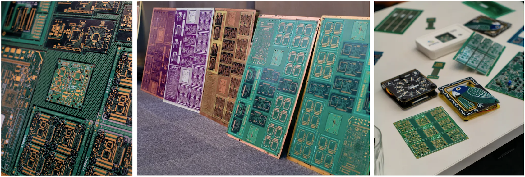
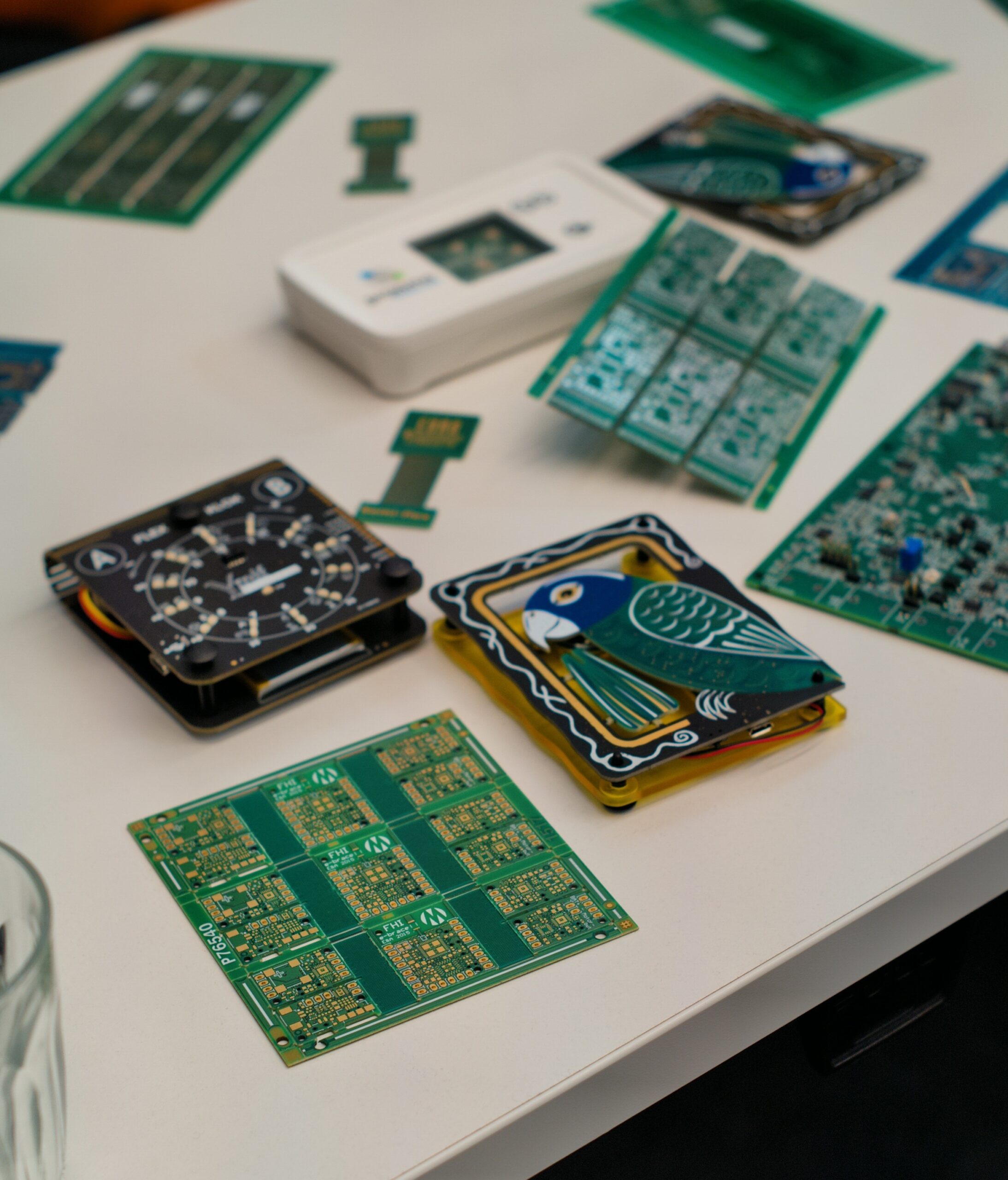
 Images: (1) Close view of a PCB boards, (2) View of different PCB boards being assembled into one manufacturing panel. Eurocircuits’ strategy to allow small-scale production at reasonable price, (3) Examples of different PCB boards types. Credit: Aude Vuilliomenet
Their presentations covered a range of topics, from the nuances of PCB manufacturing to the complexities of global supply chains. One particularly interesting aspect was their insights into how the industry is evolving to accommodate smaller production runs, making it more feasible for independent inventors and small companies to bring their products to market. They also touched on the importance of quality control in manufacturing and strategies to ensure components stocks levels and product integrity.
Most people in the electronics and fabrication industry would have acquired this knowledge from experience, tacit knowledge transfer, and sometimes common sense. Or as anyone working in hardware companies would probably say:
“We learnt it the hard way; hardware is hard — that’s why it’s called hardware.”
From reality to practice
After spending most of our mornings in the lecture hall familiarising ourselves with the concepts and the reality of making products, we were eager to break for lunch. These breaks provided opportunity for lively debate amongst ourselves.
We questioned each other about our preferred CAD software (KiCad, Fusion360, Altium, or EasyEDA?), how to choose PCB manufacturing partners, and the factors that might be influencing those choices, such as costs, IP protection, and customer support. We debated the merits of ordering PCBs with or without SMD component assembly and exchanged about experiences with various 3D printing filaments like ABS, ASA, Carbon, Conductive, PLA, and Wood. We also pondered whether final products could be 3D printed or if it CNC machining or injection moulding should be prefered.
 Images: (1) Andreas Polydorides and James Frederick Hahn preparing to solder SMD components, (2) A soldered Gamepad with micro:bit (3) Aron Eggens and Yun-Hang Cho showing their soldered Gamepad. Credit: Aude Vuilliomenet
It was a welcome change of pace to spend the afternoons in the laboratory rooms, engaging in a variety of hands-on sessions. Being in Lancaster, it perhaps came as no surprise that all of these sessions were somehow related to the user-friendly micro:bit and its plug-and-play hardware accessory system, Jacdac [4, 5].
The practical sessions were delivered by researchers John Vidler, Kobi Hartley, Lorraine Underwood, and PhD student Aron Eggens from the Computing and Digital Systems group. Building progressively from one practical to the next, we covered PCB design with KiCad, hands-on soldering of SMD components, and micro:bit programming.
There was, however, an added twist to this series of tutorials: our soldering prowess and creative coding skills were being put to the test. Mastering these skills would grant us the privilege of controlling the disco lights during the concert by the band “The Usuals” on the final evening. Making mistakes meant we would have to content ourselves with the colour choices and patterns of others. Needless to say, this little challenge kept us focused.
Demo Time
With our gaming controllers soldered and our micro:bits programmed, we were primed to dance and demonstrate our skills at the gig. However, it’s worth mentioning the other demonstrations that took place during the summer school — those of our own prototypes.
 Images: (1) Series of remote monitoring solar system unit by Matthew Little, (2) Jonas Beuchert discussing with Hassan Shahzad about his low-cost, low-power automated vision insect monitoring system, (3) Yaman Kalaji showing the PCB board inside his e-paper smart watch. Credit: Aude Vuilliomenet
To participate in this summer school, we had each submitted a short paper describing our prototype, complete with pictures and sketches, ideas for future iterations, and a responsible innovation statement addressing the sustainability and ethics of our device. During the coffee break on the second afternoon, we found ourselves back in the Sky Lounge with our prototypes occupying the tables scattered around the room.
The array of projects on display was truly impressive. Among them was a teddy bear with an interactive robotic arm designed to alleviate loneliness, units for remotely monitoring solar home systems, boards for an e-paper and power-harvesting smartwatch, and a customisable 3D-printed oral brace to assist with mindful eating and health monitoring.
These are only a few examples of the diversity and creativity of the ideas brought to life by the participants. It was inspiring to see how each participant had applied their knowledge and expertise to address real-world challenges through design and technology.
Projects from all participants can be found with detailed information on the Pro2 Network+ website.
Wrapping Up
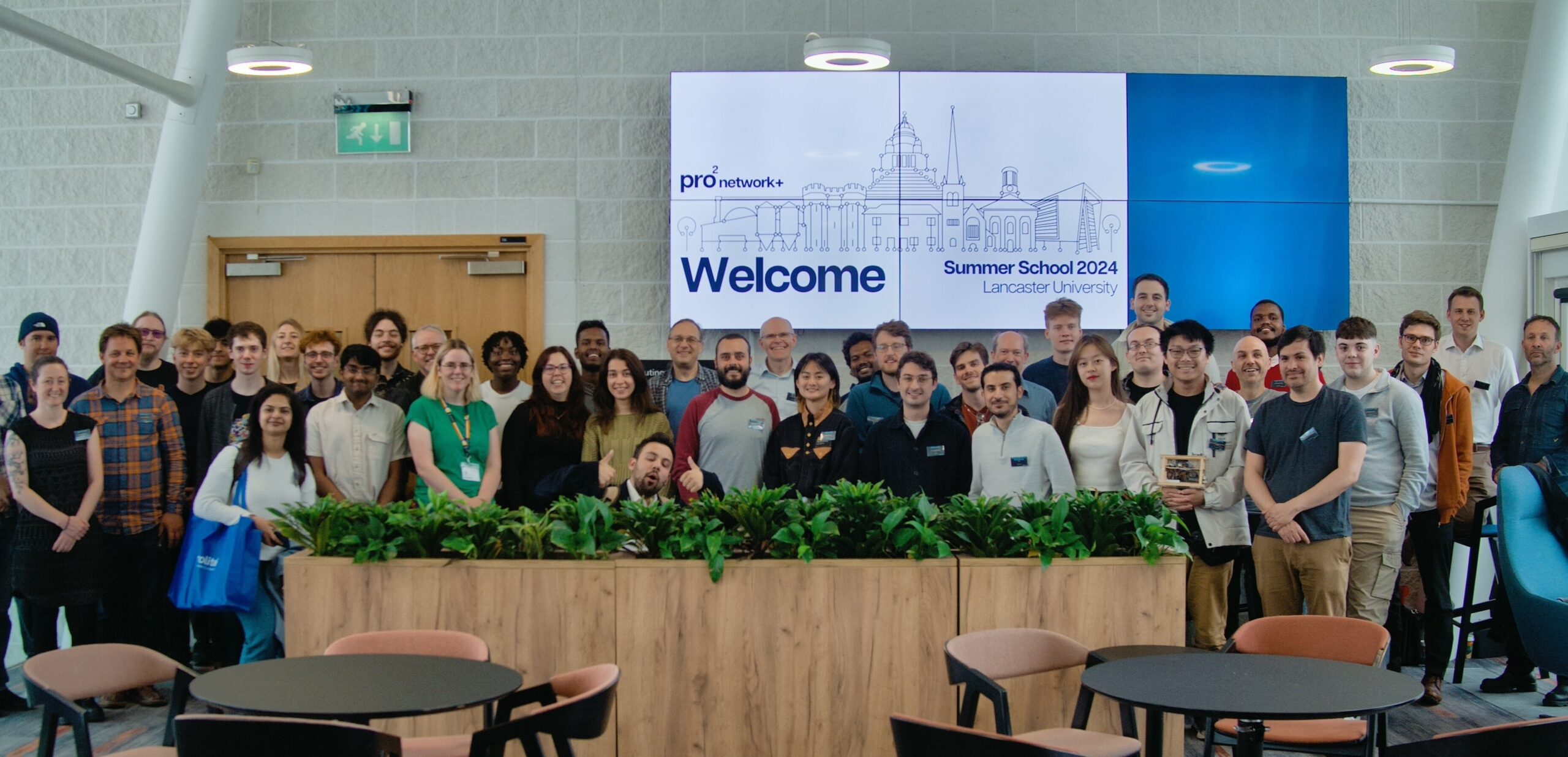
 Image: Participant, instructors, and presenters of the Pro2 Summer School 2024, Credit: Aude Vuilliomenet
Reflecting on these 72h, it’s clear that the experience was both enlightening and inspiring. We arrived with prototypes and left with a deeper understanding of the intricate process of bringing a product to life.
As we are returning to our respective projects, and I am making my way back to the Connected Environments Lab, I carry with me not only new skills and knowledge but also the spirit of collaboration and innovation that defined our time in Lancaster. The road from prototype to product may be complex. But, when encountering my next challenge and being face with questions from students, I will probably recall the learnings and experience of this summer school, and find answers and ease to them.
Thank you to the Pro2 Network+ Team.
References
[1] Hodges, S. and Fraser, M., 2022. Citizen Manufacturing: Unlocking a New Era of Digital Innovation. IEEE Pervasive Computing, 21(3), pp. 42–51. doi: 10.1109/MPRV.2022.3187574
[2] Hodges, S. and Chen, N., 2019. Long tail hardware: Turning device concepts into viable low volume products. IEEE Pervasive Computing, 18(4), pp.51–59. doi: 10.1109/MPRV.2019.2947966
[3] Anderson, C., 2007. The long tail: How endless choice is creating unlimited demand. Random House.
[4] Austin, J., Baker, H., Ball, T., Devine, J., Finney, J., De Halleux, P., Hodges, S., Moskal, M. and Stockdale, G., 2020. The BBC micro: bit: from the UK to the world. Communications of the ACM, 63(3), pp.62–69. doi: 10.1145/3368856
[5] Ball, T., de Halleux, P., Devine, J., Hodges, S. and Moskal, M., 2024. Jacdac: Service-based prototyping of embedded systems. Proceedings of the ACM on Programming Languages, 8(PLDI), pp.692–715. doi: 10.1145/3656405
Disclaimer: This article was first published on Aude Vuilli’s Medium Blog in July 2024.


